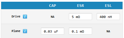
The parameters under Plane defines the power plane pair characteristics.This is simulated using the two parameters CAP and ESR. Capacitance and DC resistance. Enter CAP in micro Farad (uF) and ESR in mili-ohm.
To determine the right values to use for CAP and ESR, the best thing obviously is measurements. The next best thing is some simple formulas.
Capacitance (CAP)
The capacitance of a parallel plate capacitor of area A and with a distance between the plates of d is given by this formula.

where,


Examples
| Prepreg | Dk | um | 50×100 mm | 100×100 mm | 100×200 mm | 200×200 mm |
| 106 | 4.0 | 50 | 3.6 nF | 7.3 nF | 14.5 nF | 29 nF |
| 1080 | 4.2 | 63 | 2.9 nF | 5.8 nF | 11.5 nF | 23 nF |
| 2125 | 4.3 | 100 | 1.8 nF | 3.6 nF | 7.3 nF | 14.5 nF |
| 2116 | 4.4 | 125 | 1.5 nF | 2.9 nF | 5.8 nF | 11.6 nF |
Conversion help: 1nF = 0.001uF, 25.4 mm = 1″ and 25.4um = 1 mil
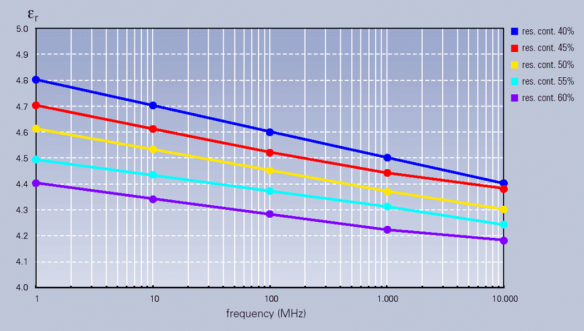
Note the dielectric constant is not really a constant, as it varies with frequency, temperature and other parameters. This is illustrated by the below example graph. You should find the values in the datasheet for the actual material used.
Equivalent Series Resistance (ESR)
Can often be set to 0 ohm.
Rolf,
For your PDN Tool it would be nice if you could include a plane to plane capacitor calculator.
Examples online include:
http://www.daycounter.com/Calculators/Plate-Capacitor-Calculator.phtml
http://www.calctool.org/CALC/eng/electronics/parallel_plate
best regards,
Randy Clemmons CID+
An observation: The more plane capacitance, the lower the plane resonance frequency. This leads me to think, that if we can reduce capacitance (eg. by reducing plane area) while keeping ESL low (short via length, optimal footprints), we’ll get the best results. What are your thoughts on this, Rolf?
In some way right, but you also have a minimum amount of charge needed for the ICs at every switching event. This charge will (initially) have to come from the on-die/package and PCB plane capacitance. This sets the minimum plane capacitance required.